Basics of Digital Electronics Part 3
Binary Addition
As we did in the 2nd Part that logic gates are made from the transistors. Truth table of all the gates is shown in the image.
In this part I will show you that how binary addition is done using these gates. Addition of two bits is shown below
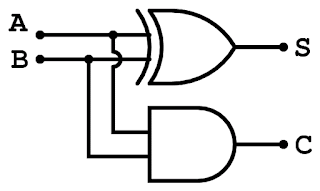
3rd column in above table shows the sum of two bits A and B. If we look in the image then column 3 represents the truth table of XOR gate. similarly 4th column which shows the carry out represents the truth table of AND gate.
Therefore expressions for sum and carry becomes
Sum = A XOR B
Carry = A AND B
So we can implement it using two gates( XOR gate and AND gate). The circuit diagram for this is shown below.
This circuit takes the two inputs or two bits A , B and gives the sum and carry as an output. But it doesn't take carry in as an input. That is why it is known as Half Adder. We can't use this circuit in parallel with similar circuits for 2,4,8... bit addition.
To solve this problem another circuit known as Full Adder was designed. First we will look at the table.
This circuit takes the three inputs. Input A, b and Carry In and gives two outputs Sum and Carry out. Expression for sum and carry can be solved using K map technique.
This logic can be implemented by the following circuit where c represents the carry in or Cin.
Advantage of this circuit is that we can use it for multi bit addition by connecting the Cout of 1st unit to Cin of 2nd unit and Cout of 2nd unit to cin of 3rd and so on.
where P0,P1,P2,P3 are the four four bits of 1st quantity(1010) and Q0,Q1,Q2,Q3 represents the four bits of 2nd value. S0,S1,S2,S3 represents the four bit Sum. CI is carry in of 1st unit and CO is carry out of the last unit.
IC 7483 is used as four bit full adder and pin diagram of this IC is shown below.


Comments
Post a Comment